Research of nanoparticle fabrication and nanoscale characterization on dielectrics
Keigo Suzuki
Title on original paper: Research of nanoparticle fabrication and nanoscale characterization on dielectrics
Reference
- Keigo Suzuki and Kazunori Kijima, "Effect of oxygen injection on synthesizing barium titanate nanoparticles by plasma chemical vapor deposition", J. Mater. Sci. 41 (2006) 5346-8.
- Keigo Suzuki and Kazunori Kijima, "Dielectric properties of BaTiO3 films prepared by RF-plasma chemical vapor deposition", Jpn. J. Appl. Phys. 44 (2005) 8528-35.
- Keigo Suzuki, Keisuke Kageyama, Hiroshi Takagi, Yukio Sakabe and Kazuo Takeuchi, "Fabrication of monodispersed barium titanate nanoparticles with narrow size distribution", J. Am. Ceram. Soc. 91 (2008) 1721-4.
- Keigo Suzuki, Nobuhiko Tanaka, Keisuke Kageyama and Hiroshi Takagi, "Fabrication of well-dispersed barium titanate nanoparticles by the electrospray of a colloidal solution", J. Mater. Res. 24 (2009) 1543-52.
- Keigo Suzuki, Takafumi Okamoto, Hiroyuki Kondo, Nobuhiko Tanaka and Akira Ando, "Insulation degradation behavior of multilayer ceramic capacitors clarified by Kelvin probe force microscopy under ultra-high vacuum", J. Appl. Phys. 113 (2013) 064103.
Presentation media: The Ceramic Society of Japan, Award lecture of 68th CerSJ Awards for advancements in industrial ceramic technology
The recent miniaturization of high capacitance multilayer ceramic capacitors (MLCCs) expedites not only thinning the dielectric layers on MLCCs but also downsizing the grains in the dielectric layers. Assuming further thinning trend prevails in the near future, it is crucially important to establish fabrication methods of dielectric nanoparticles with particle sizes of around 10 nm as well as to clarify the effect of grain sizes on the dielectric properties. We developed fabrication methods of barium titanate nanoparticles with particle sizes of around 10 nm by gas-phase process and investigated the dielectric properties of the obtained nanoparticles. The thinning trend also requires the precise design of dielectric layers, thereby the characterization of dielectric layers from microscopic point of view and its feedback to the material design will be one of the important approaches. In particular, it is vitally important to secure reliability on thin dielectric layers. In this research, we investigated insulation-degradation mechanism of dielectric layers by using scanning probe microscope under ultra-high vacuum as a characterization method in nanometer region.
Fabrication of dielectric nanoparticles
The recent miniaturization of high capacitance multilayer ceramic capacitors (MLCCs) accelerates thinning trend of dielectric layers. The dielectric layers usually consist of several grains to secure the reliability on MLCCs, which results in the size reduction trend of the grains in dielectric layers. This trend demands the downsizing of powder raw materials of dielectrics. When we consider how to grapple with further thinning trend, it will be crucially important to fabricate dielectric nanoparticles with particle sizes of around 10 nm and to evaluate their dielectric properties as well. Barium titanate (BaTiO3) is one of the major ferroelectric materials that are used in MLCCs. In this research, we have established the fabrication methods of BaTiO3 nanoparticles with particle sizes of around 10 nm based on the gas-phase processes such as plasma CVD, laser ablation, and electro-spray method.
Inductively coupled plasma (ICP) is used in the plasma CVD method. This method has following advantages; (1) The raw materials are decomposed to atomic levels due to the high temperature in ICP. The ultrafine particles can be fabricated since the nucleated particles in the gas stream are quenched from high temperature region. (2) The nanoparticles with high purity can be obtained since an electrodeless discharge prevents contaminations being mixed into the nanoparticles. Since there had been no examples of fabricating BaTiO3 nanoparticles using ICP and no instruments as well, we launched design and assembling of the instrument for our research. In this method, nanoparticles are fabricated by introducing Metallo-organic gas mixture of barium and titanium into the ICP. By optimizing experimental parameters such as gaseous pressure, gas flow rate, and the position of oxygen introduction, we eventually succeeded in fabricating BaTiO3 nanoparticles with average particle sizes less than 10 nm (Figure 1). The electron diffraction pattern demonstrates that the nanoparticles have perovskite structure in spite of being ultrafine.
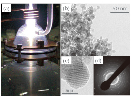
Figure 1 (a) Appearance of the fabrication of BaTiO3 nanoparticles by plasma CVD, (b) TEM bright field image of the fabricated naoparticles, (c) TEM lattice image of the fabricated nanoparticles, (d) selected area electron diffraction pattern of the fabricated nanoparticles.
The nanoparticles obtained by the plasma CVD are not well dispersed but has a broad size distribution since the nanoparticles easily aggregate by undergoing high temperature region. To resolve the problem, we tried laser ablation and electro-spray method. In the former method, nanoparticles are nucleated in the gas stream just after vaporizing BaTiO3-ceramic target by pulsed laser irradiation. The nanoparticles are then introduced into the tubular furnace for crystallization. By selecting the crystallized nanoparticles with specific particle size using differential mobility analyzer, well-dispersed nanoparticles with uniform particle sizes can be obtained. In the latter method, the solution that contains barium and titanium elements is continuously supplied to capillary. The electrically-repulsive ultrafine droplets are generated by applying a high voltage to the capillary. The well-dispersed BaTiO3 nanoparticles can be obtained by vaporizing solvents from the droplets through annealing in the tubular furnace. By optimizing fabrication conditions in both methods, well-dispersed BaTiO3 nanoparticles with particles sizes of around 10 nm were successfully fabricated as shown in Figure 2. Above methods are not necessarily available for mass production. However, the obtained BaTiO3 nanoparticles are suitable for investigating its intrinsic properties since the nanoparticles are well-dispersed and have a narrow size distribution. We expect that the obtained nanoparticles will serve to establish the design guideline of dielectric nanoparticles for future MLCCs.
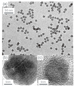
Figure 2 (a) TEM bright field image of BaTiO3 nanoparticles fabricated by laser ablation, (b) TEM lattice image of the fabricated nanoparticles, (c) TEM lattice image of BaTiO3 nanoparticles fabricated by electro-spray method.
Dielectric properties of BaTiO3 nanoparticles
We investigated dielectric properties of BaTiO3 nanoparticles synthesized by plasma CVD. The Pt/Si substrate was placed in the tail flame of ICP. Since the change in the distance between the substrate and the center of ICP can alter substrate temperatures, the morphology of thin films can be controlled from columnar to granular fashions. In this way, we fabricated nanocrystalline thin films. The grains in the films were adjusted to various sizes by post-annealing the films using rapid-thermal annealing furnace. Subsequently, the capacitor structure was made by forming upper Pt electrodes using sputtering. Figure 3 shows grain size dependence of relative permittivity (εr) measured under AC 100 mV and 1 kHz. This figure also shows the c/a lattice constant ratios of plasma-CVD-derived BaTiO3 nanoparticles estimated by Rietveld analysis from XRD patterns. In the size region of around 50 nm, the εr and c/a are found to be approximately 1000 and 1.005, respectively. Further, we investigated not only P-E hysteresis and DC-bias voltage dependence of capacitance for nanocrystalline films but also Raman spectroscopy and latent heat on phase transition for nanoparticles. As a result, we found that tetragonal structure and ferroelectricity maintained at the grain sizes greater than 30 nm. In general, a size reduction in ferroelectrics annihilates ferroelectricity, which results in the decrease of εr due to the size effect. However, the present experiment demonstrates the possibility that high εr value can be kept in the ultrafine particles. These results indicate that BaTiO3 has a great potential even in the small size region. This fact is expected to become the guideline when thinning dielectric layers in MLCCs.
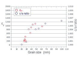
Figure 3 Grain size dependence of relative permittivity (εr) for BaTiO3 nanocrytalline films fabricated by plasma CVD measured under AC 100 mV and 1 kHz. The figure also shows the c/a lattice constant ratios of plasma-CVD-derived BaTiO3 nanoparticles estimated by Rietveld analysis from XRD patterns.
Nanoscale characterization on dielectrics
Above-mentioned evaluations such as XRD and dielectric properties are based on the average information obtained from numerous grains. In reality however, the properties of individual grains seem to be different. Factors such as grain boundary, electrode/dielectric interface, and so on should significantly affect the properties. In light of these facts, not only the macroscopic evaluations but also the measurement techniques of material properties from microscopic point of view will be vitally important in order to finely design dielectric materials. As a nanoscale characterization method on dielectrics, we used scanning probe microscope under ultra-high vacuum (UHV-SPM). This method has following advantages; (1) we can investigate intrinsic properties of materials since clean material surface is obtained by the benefit of UHV environment. (2) we can measure the properties with high accuracy owing to high spatial and high energy resolution of the instrument. The research on dielectric materials using UHV-SPM is one of the unexplored fields. Thereby, this technique has a high potential to offer new knowledge on dielectrics. There are many attractive measurement modes in SPM. In this paper, we introduce the evaluation of insulation degradation on MLCCs using Kelvin probe force microscopy (KFM).
High capacitance of MLCCs can be realized by thinning dielectric layers. However, the thin dielectric layers are subject to a high electric field when applying a DC voltage, which leads to dielectric breakdown even under the usage less than rated voltage. This indicates that securing the reliability on MLCCs is quite difficult when thinning dielectric layers. In particular, an addition of acceptor elements for the sake of reduction-resistant properties forms oxygen vacancies in dielectric layers. It is commonly recognized that these oxygen vacancies migrate through ceramic grains under the DC electric field and eventually cause insulation degradation. Thus far, the major approach for investigating degradation mechanisms focuses on macroscopic methods such as impedance analysis etc. The microscopic characterizations for the degraded dielectrics have been scarcely reported. KFM is the method to measure the surface potential of materials by using conductive tip with curvature radius of the order of nanometer. Surface potential distributions on the channel of working organic thin film transistor have been evaluated by applying a DC bias voltage to the lateral direction of the device. In this research, the analogous measurement was implemented by applying a DC bias voltage to dielectric layers in MLCCs to investigate the distributions of resistance, i.e. surface potential gradient. We can get highly reliable data since the effect of atmospheric components such as water on surface potentials can be ruled out by the benefit of UHV measurement of approximately 10-8 Pa.
The HALT (100 h, and 215 h) for MLCC (X5R, 2.2μF, 4.2 × 1.6 × 1.6mm3, 3.8μm of dielectric layer) was conducted under the condition of 150 ºC and 40 V. The resistances of the 100 h-degraded sample and the 215 h-degraded sample were 0.6 and 2.2 orders of magnitude lower than the sample without HALT (fresh MLCC), respectively. The samples were mirror-polished on faces perpendicular to the inner electrodes and then mounted on sapphire substrates. The external electrodes of MLCC were wired to a DC power supply using silver paste. Regarding the degraded samples, the cathode in HALT was grounded while the external DC bias voltage of +5V (forward bias) or –5V (backward bias) was applied to the anode in HALT. The measurement based on non-contact mode was performed using PtIr5-coated conductive tip under room temperature.
Figure 4 shows line profiles of surface potential on dielectric layers investigated by KFM measurement. Dielectric layers show clear voltage drops while the gradient of the surface potential in the Ni inner electrode is approximately zero. We can see a step-like voltage drop in the dielectric layer of the fresh MLCC. The steps of the voltage drop in 100 h-degraded sample turn into a fine structure. Eventually, these fine steps in voltage drop almost disappear in 215 h-degraded sample. In general, the resistance of grain boundaries is greater than that of grains. It is speculated that high insulation resistance of grain boundaries on the fresh MLCC is responsible for the clear voltage drops. These voltage drops seem to disappear due to a decrease in resistance of grain boundaries with the evolution of degradation. We believe that the KFM measurement was capable to detect these phenomena; however we need further research to totally understand the behavior.
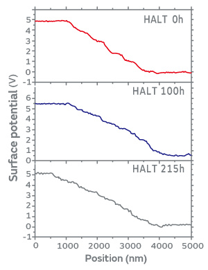
Figure 4 Line profiles of surface potential on dielectric layers investigated by KFM measurement under the forward bias
Figure 5 shows electric field images for the cross sections of MLCCs. These images were derived by differentiating surface potential images in a thickness direction of dielectric layers. The Ni electrodes and the dielectric layers are located on both sides and centers of each figure, respectively. The measurements of both forward and backward bias were implemented at the same position in each sample. In case of the fresh MLCC, we can see no characteristic behavior on the interface between Ni electrodes and dielectric layers under the both bias voltages. On the other hand, the electric field concentration is found in dielectric layers near the anode (the cathode in HALT) for the 100 h-degraded sample at the backward bias voltage. This concentration becomes much significant in the 215 h-degraded sample. In case of the forward bias voltage however, the electric field is distributed homogeneously in the 100 h-degraded sample. A certain degree of electric field concentration comes to appear near the anode (the anode in HALT) in the 215 h-degraded sample. These phenomena were similarly found in the different areas.
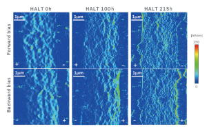
Figure 5 Electric field images for the cross sections of MLCCs. The Ni electrodes and the dielectric layers are located on both sides and centers of each figure, respectively. These images were derived by differentiating surface potential images in a thickness direction of dielectric layers. The notations “+” and “–” shown in Ni electrodes represent positive and negative potentials, respectively. The measurements of both forward and backward bias were implemented at the same position in each sample.
According to consideration based on the energy band diagram, the energy barriers and resultant high resistances formed in the vicinity of the anode give rise to electric field concentrations if we assume that the degraded dielectric layers are p-type semiconductors. This consideration is consistent with the results of the present study, suggesting that the electric field concentrations formed in the vicinity of the anode in HALT lead to the insulation degradation. It will be important to clarify the conduction type of the degraded dielectrics in the future. The band diagram also suggests that band bending near the cathode in HALT leads to high resistance when the oxygen vacancies are accumulated at the cathode. In this study, the electric field concentration was much remarkable near the anode at backward bias, i.e. the cathode in HALT. This phenomenon may originate from oxygen-vacancy migration that is a dominant factor in the degradation. These findings regarding insulation-degradation mechanism obtained from the microscopic evaluations will be beneficial for the design of dielectric layers that have high reliabilities.
Conclusion
We established fabrication methods of BaTiO3 nanoparticles with particles sizes of around 10 nm using gas-phase process. In particular, the dielectric properties with grain size regions of several tens nanometer were clarified by using BaTiO3 nanoparticles derived from plasma CVD. We also demonstrated that the nanoscale characterization using UHV-SPM is available for the dielectric materials. If we further apply various functions of SPM to the nanostructures of dielectrics, the resultant new knowledge will greatly contribute to the materials design for the future MLCCs.
Glossary
*1 c/a lattice constant ratio:
The lattice constant ratio of c-axis to a-axis in the tetragonal perovskite structure. This ratio is used as an index that represents the degree of ferroelectricity in BaTiO3 powder. The c/a of bulk BaTiO3 of tetragonal structure at room temperature is 1.011.
*2 HALT:
An abbreviation for Highly Accelerated Lifetime Test. This is the accelerated lifetime test to evaluate the reliability on MLCCs by applying a DC voltage greater than rated voltage under high temperature.
*3 KFM measurement:
A method to measure surface potentials based on Kelvin probe Force Microscopy. In this measurement, DC and AC voltages with angular frequency ω are simultaneously applied to the conductive tip. The surface potentials are investigated by controlling DC voltages so as to nullify w vibration signals that originate from electrostatic force between tip and sample.