Development of High-Accuracy Automotive Circuit Boards Using LFC® Substrates
Junzo Fukuta, Seigo Oiwa, Masashi Fukaya, Hideaki Araki
Original Paper: Development of High-accuracy Automotive Circuit Boards Using Low-temperature Co-fired Ceramics Ceramics Japan 47 (2012) , pp.550-551
References
Original Papers:
- S.Nishigaki, S.Yano, J.Fukuta, M.Fukaya T.Fuwa, ISHM (1985) 225-234
- S.Nishigaki, J.Fukuta, S.Yano, H.Kawabe, K.Noda, M.Fukaya, ISHM (1986) 429-449
- M.Fukaya, T.Matsuo, S.Nishigaki, C.Higuchi, ISHM (1997)
- M.Fukaya, C.Higuchi, IMAPS (2000) 636-641
Electronic control in automobiles began to come into widespread use from 1980s. Because reliability over long periods of time was required, components were mounted on substrates made of ceramic materials, particularly HIC® substrates that combined Ag-based conductor materials and RuO2-based resistor materials with an alumina substrate as the base.
Soon, advancements in control led to more expansive circuits, resulting in larger substrate sizes, leading to a need for multilayer substrates.
As a result, Murata Manufacturing's LFC® (low temperature fireable ceramics) substrate, which is a type of LTCC (low temperature co-fired ceramics) substrate using Ag and RuO2 based materials, began to attract wide attention.
LFC® substrates use the same conductor and resistor materials having a proven track record in HIC® substrates, use co-firing for high insulation reliability, and use non-shrinkage firing unique to LTCC substrates for providing high dimensional accuracy. These substrates entered the automobile market in 1994, and today, they are widely used, particularly by automotive electrification equipment manufacturers in the United States and Europe.
What Are LTCC Substrates?
LTCC, or low temperature co-fired ceramics, get their name because they are ceramics that allow multilayer co-firing with conductors at a relatively low temperature of 800°Cto 1,000°C, and they typically use a mixture of glass and filler material.
One major feature of LTCCs is that non-shrinkage firing uses the fluidity of glass for enabling high dimensional accuracy and flatness and that conductor materials with high conductivity and relatively low melting points such as Ag, Cu, and Au can be used.
Although a wide range of LTCC substrates have been developed, this paper covers the LFC® substrate developed exclusively by Murata Manufacturing and examples of its automotive in-vehicle applications.
What Is Non-Shrinkage Firing?
Normally, ceramics shrink in the three directions of length, width, and thickness during firing. Shrinkage of about 20% occurs in each direction, but poor dimensional accuracy and warping can occur due to density variation in the multilayered body, shrinkage occurring at different times with the conductors, temperature variation within the furnace, friction between the fired piece and its support, and other factors.
The dimensional accuracy and flatness of the ceramic substrate is important in processes where semiconductors and other components are mounted, and non-shrinkage firing technology was developed as a solution to this issue.
Non-shrinkage firing is a method that applies a constraining force to the front and back of the sintered object during firing so that shrinkage occurs in the thickness direction only without any shrinkage in the planar direction. Alumina or similar material that does not sinter at the LTCC firing temperature is used for the constrained layer. This is a technology that is not possible in alumina-based HTCC (High Temperature Co-fired Ceramics) that is used as packages for ICs, crystal units, and other components.
The pressurized method (LFC® substrates in this paper) where firing is performed while applying pressure, non-pressurized method where no pressure is applied, and the non-pressurized self-non-shrinkage method that does not use an external constrained layer are being devised. Each method has its own unique features, but the pressurized method in particular enables superior flatness. Figure 1 shows a comparison of the flatness of LFC® testing substrates created using the pressurized method and the non-pressurized method. Figure 2 shows a conceptual diagram of the pressurized method.
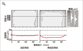
Fig. 1 Comparison of Flatness in Pressurized Method and Non-Pressurized Method
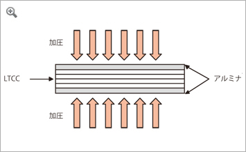
Fig. 2 Pressurized Non-Shrinkage Firing
Development of LFC® Substrates
The late Dr. Susumu Nishigaki was a driving force in the development of LFC® substrates as LTCC substrates that did not contain toxic substances such as Pb, Cd, and Cr.
LFC® substrates are ceramics consisting of CaO-Al2O3-SiO2-B2O3 based glass and Al2O3 filler. These substrates feature high strength and chemical stability by using the precipitation of anorthite as the crystalline phase. When announced at ISHM* in 1985 and 1986, these papers received the Best Paper awards and other distinguished honors.1) 2)
To enable co-firing with an Ag conductor, precise control of Ag particles is used to match the shrinking times and obtain adhesion strength and high-quality printing characteristics. RuO2 based resistors can also be formed on the surface, but to improve reliability for use in automotive applications, material development was conducted with particular focus on differences in thermal expansion with the substrate, and in temperature cycle testing from -40°Cto+150°C, the variation was held to ±1% or less even after 3,000 cycles.3) 4)
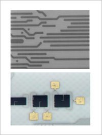
Photo 1 Example of L/S=125µm/125µm Internal Layer Ag Conductors and Printed Resistors
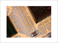
Photo 2 Example of Plating Surface and Au Wire Bonding
Because the substrate does not contain Pb, it is highly resistant to acidic and alkaline treatments, easily enables electroless chemical plating, and enables Ni/Au plating on Ag conductors because of its solder resistance and support for wire bonding on bare chips. Furthermore, Ni/Pd/Au plating is possible in cases where thermal resistance is required for enabling production of environmentally-friendly and low-cost substrates without using the traditionally high-cost Au or Ag/Pd thick film conductors.
- The features of LFC® substrate systems are shown below.
- High dimensional accuracy ±0.05%
- Excellent flatness 5µm/4mm square
- Support for large panel production 8-inch square
- Plating applications Ni/Au, Ni/Pd/Au (Wire bonding is possible)
- Surface printed resistors Accuracy±1% (after trimming) TCR 0±100ppm/°C
- Environmental friendliness Pb, Cd, and Cr-free
Development for Automotive Applications
LFC® substrates first appeared as VCO (voltage controlled oscillator) substrates for mobile phones in 1986, but once the breakthroughs mentioned before were announced at ISHM, automotive ECU (electronic control unit) substrates for ABS (anti-lock braking systems) , that is, electronic control substrates, were adopted by European automotive electrification equipment manufacturers. Soon, installation of these components became standard among many automobile manufacturers around the world, and since 1994, more than 200 million have been produced. Recently, they have become more widely used as automotive ECU substrates for engine management, transmission control, power steering, and other applications. In transmission control, these substrates have been used by German luxury car manufacturers for the control of 7-speed automatic transmission, and since their launch in 2003, their production has reached 5 million units. Ceramic substrates, particularly LFC® substrates, are used because these substrates are installed in locations subjected to high temperatures and vibrations within the engine room.
A conceptual drawing (cross-section) of an automotive LFC® substrate is shown in Fig. 3. The substrate in this example has a structure where the components are mounted on one side of the substrate, printed resistors are arranged on the back surface with resistance values adjusted by laser trimming, and heat generated by the installed components is dissipated to the back surface by thermal vias. These substrates have a large size of approximately 50mm square and contain a large number of mounted components and wire bonds. For this reason, the dimensional accuracy and flatness of the substrate are important factors during mounting, and the characteristics of pressurized non-shrinkage firing are most suited for these requirements. In contrast to the conventional HIC® substrate, printed resistors are arranged on the back surface for also contributing to more effective usage and compact design on the back surface.
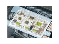
Photo 3 Example of Components Mounted on Automotive ECU Substrate
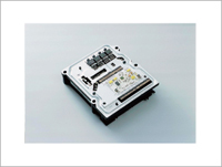
Photo 4 ABS Module
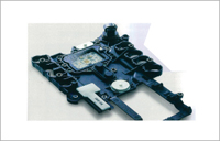
Photo 5 Transmission Control Module
In the substrate mounting example shown in Photo 3, conductive glue is used to mount bare chip ICs, capacitors, and other components on the LFC® substrate, Au wire bonding is used to connect with the IC, and Al wire bonding is used to connect with external input/output terminals.
Photo 4 shows an actual ABS module, and Photo 5 shows a transmission control module.
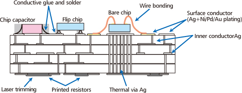
Fig. 3 LFC® Substrate Structure for Automotive ECU Substrate
Conclusion
In coming years, control modules with even higher densities and higher reliability are expected to be developed to meet the needs for higher fuel efficiency and comfort through advanced communication control and more lightweight car bodies.
The LFC® substrate is a mounting substrate that meets these various requirements, but looking ahead, an important issue will be price competition with printed circuit boards (PCBs) which are expected to support large currents and have enhanced resistance to heat.
*ISHM: Abbreviation for the International Society for Hybrid Microelectronics. The Japan headquarters was established in 1967. In 1998, the ISHM merged with the Institute of Printed Circuits to start the current Japan Institute of Electronics Packaging (JIEP) .