4-1. Introduction
When using an EMI probe to measure the distribution of noise in order to implement noise suppression measures, there is sometimes a high amount of noise throughout the entire board, making it difficult to diagnose. You may think that this is caused by the resolution of the EMI probe being poor, but in many cases there is simply noise throughout the entire board. In addition, noise from a board will also propagate and spread to cables connected to the board.
There are two major reasons why noise spreads and propagates on a board like this. First, this can be caused by the return current of harmonic noise from a signal propagated over a transmission line spreading and propagating to ground (GND). Second, this can be caused when metal is exposed to the magnetic field generated by a noise current, generating an induced current which causes the magnetic field to be reradiated.
We used a 3D electromagnetic field simulator to visualize the propagation of the noise current and magnetic field.
 Figure 1. Example results of measuring magnetic field distribution on a board
4-2. Return current spreading to GND
First, we visualize the return current of harmonic noise spreading and propagating to GND.
4-2-1. Simulation model
The microstrip line shown in Figure 2-1 is used as our simulation model. A 1 GHz harmonic is included in the signal to function as noise. The skin effect causes the current to be concentrated on the surface of the conductor in such a high frequency. The current will particularly concentrate on a surface where the transmission line and GND face each other, so we simulated current and a magnetic field on the following surface.
(1) GND side of transmission line
(2) Transmission line side of GND
Figure 2-1. Simulation model
(Microstrip line)
4-2-2. Results of current density simulation
The results of simulating current density flowing along the transmission line and GND are shown in Figure 2-2.
The animation shows the transient and steady states from when noise begins propagating. These results reveal the following about noise propagation:
- Noise current on the transmission line gradually propagates toward the load side.
- As with on the transmission line, noise current on GND also propagates toward the load side.
- Current on GND is strong directly beneath the signal line and spreads out from there.
In other words, noise current propagates to the load side on both the transmission line and GND.
Changes in current density (animation)
Maximum current density value
Figure 2-2. Results of current density simulation
(load 50 Ω, 1 GHz)
4-2-3. Why noise current spreads on GND
When considering direct current, the general belief is that current would flow in a loop over the load to GND. However, current on GND propagates gradually toward the load side (similar to current on the transmission line), and not in a loop (as with direct current). The reason why follows.
A simple equivalent circuit for a microstrip line is shown in Figure 2-3. There is inductance (L) in the transmission line, and capacitance (C) in the area between the transmission line and GND. DC resistance in the transmission line and GND, and inductance in GND, are sufficiently small to be omitted here. High-frequency current flows in a loop along L and C, as it propagates from the transmission side to the load side. Therefore, current on GND also propagates gradually toward the load side.
 Figure 2-3. Microstrip line equivalent circuit
The results of simulating current density with the load condition open are shown here, in order to more easily show how current flows along L and C (which exist in a distributed manner), instead of in a loop along the load (Figure 2-4).
As shown here, current flows near the open end of the transmission line. These results suggest that current flows over L and C (which exist in a distributed manner).
Changes in current density (animation)
Maximum current density value
Figure 2-4. Results of current density simulation
(load open, 1 GHz)
Why does noise current spread along GND? Figure 2-5 shows the microstrip line equivalent circuit rendered three-dimensionally. Capacitance is large directly under the signal line and GND, and decreases with distance. This means that the current on GND is strongest directly beneath the transmission line and spreads out around this area.
 Figure 2-5. 3D microstrip line equivalent circuit
4-2-4. Impact of noise filter installation position
Current flows along L and C (which exist in a distributed manner), so the effect of a filter installed as a noise suppression measure will vary based on where it is installed.
This section describes how current density changes based on where a ferrite bead is installed.
We ran simulations with a ferrite bead placed on (1) the transmission side, (2) the center of the transmission line, and (3) the load side (Figure 2-6.)
 Figure 2-6. Differences in (maximum) current density value due to ferrite bead installation position
As shown here, as the ferrite bead is placed further away from the transmission side, noise on GND becomes stronger and the measure loses effectiveness. This is because noise current propagates along the transmission line up until where the ferrite bead is located, and so it also propagates similarly on GND. In other words, installing a filter on the transmission side is a more effective measure for suppressing noise sources.
4-3. Induced current caused by a magnetic field
Next, we visualize how an induced current is generated when metal is exposed to a magnetic field generated by noise current, which causes the magnetic field to be reradiated.
4-3-1. Distribution of magnetic field propagating through space
The results of simulating how a magnetic field propagates is shown in Figure 3-1.
The analysis surface includes the board itself and the air around it.
Changes in magnetic field (animation)
Maximum magnetic field value
Figure 3-1. Results of magnetic field distribution simulation
(load 50 Ω, 1 GHz)
4-3-2. Magnetic field generated by induced current from a magnetic field
When metal is exposed to the magnetic field, an induced current flows to the metal, and a magnetic field is radiated from the metal. This is called reradiation. We will visualize this here.
We simulated magnetic field distribution with a piece of metal similar to the transmission line placed in the space above the microstrip line (Figure 3-2). This was done under the assumption that a plastic case in the upper portion of the board would be reinforced with metal or contain a heatsink or other metal.
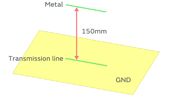 Figure 3-2. Simulation model
(dielectric not shown)
The results of the magnetic field change simulation are shown in Figure 3-3.
First, the magnetic field radiated from the transmission line heads toward the metal suspended in air. Once the magnetic field reaches the suspended metal, a magnetic field is generated in the direction of the transmission line. This is because the metal has been exposed to the magnetic field, causing induced current to flow to the metal and causing reradiation.
Thus, when metal is exposed to a magnetic field, it causes an induced current to flow, resulting in reradiation. None of this is necessary, so it is all noise.
Changes in magnetic field (animation)
Maximum magnetic field value
Figure 3-3. Results of magnetic field distribution simulation
(load 50 Ω, 1 GHz)
Among the metal exposed to a magnetic field will of course include board patterns and cables connected to the board.
These can therefore also result in noise generated by a magnetic field.
In order to check this, we added a dummy pattern (with no signal input) and a GND cable, and then simulated magnetic field distribution. Note that the analysis surface includes the board itself and the air around it.
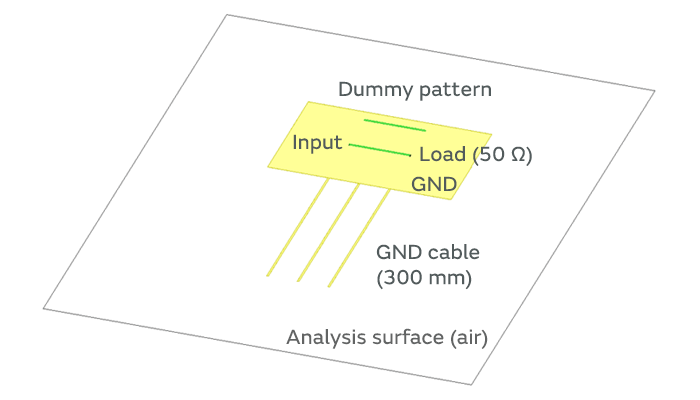 Figure 3-4. Simulation model with dummy pattern and GND cable added
(dielectric not shown)
The simulation results are shown in Figure 3-5.
Changes in magnetic field (animation)
Maximum magnetic field value
Figure 3-5. Results of magnetic field simulation with dummy pattern and GND cable added
(load 50 Ω, 1 GHz)
This shows that, when a magnetic field is generated by current on the transmission line or GND, any metal exposed to it will cause another magnetic field to be generated by induced current— in other words, noise. If we define common mode noise as common noise that propagates in the same direction and in phase with any metal present, then we can also categorize as common mode noise any noise generated when metal is exposed to a magnetic field.
4-4. Impact of GND pattern on noise
We have seen how noise current spreads to GND and how this current causes noise to propagate to any metal exposed to the magnetic field.
How noise current propagates (and therefore the condition of noise) will vary depending on board conditions. To show an example of this, we simulated a magnetic field where a slit was opened on GND directly beneath the transmission line. The simulation model is shown in Figure 4-1. Note that no slit was opened in the dielectric.
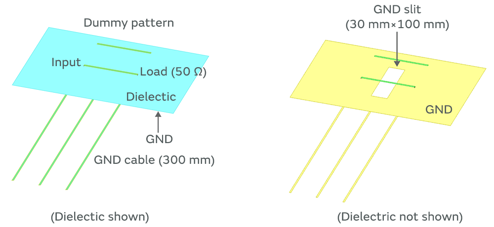 Figure 4-1. Simulation model with slit opened in GND
The results of the magnetic field simulation are shown in Figure 4-2.
Changes in magnetic field (animation)
Maximum magnetic field value (without GND slit)
Maximum magnetic field value (with GND slit)
Figure 4-2. Results of magnetic field simulation with slit opened in GND
(load 50 Ω, 1 GHz)
This shows the strength of the magnetic field radiated from the board and cable increases based on the slit shape.
The slit prevents the return current from flowing directly beneath the signal line, and the current is diverted around the slit. Due to the distance between the signal current and magnetic field, the magnetic field cancellation effect caused by reverse flowing is reduced, resulting in a stronger magnetic field. This also strengthens the magnetic field on GND, the dummy pattern, and the GND cable.
Finally, we inserted a ferrite bead on the transmission line, in order to show that the noise propagating to the board and cable is caused by the noise current input to the transmission line. The results of this magnetic field simulation are shown in Figure 4-3.
Magnetic field maximum value
(without ferrite bead)
Magnetic field maximum value
(with ferrite bead)
Figure 4-3. Results of magnetic field simulation with ferrite bead added to transmission line
(load 50 Ω, 1 GHz)
The ferrite bead reduces the magnetic field on the cable and board, confirming that current on the transmission line was the major cause of the noise.
4-5. Summary
We showed here how noise propagating along a transmission line first spreads to GND, and then spreads to the rest of the board, cables, and other components. When noise propagates along a transmission line, capacitance (C) and inductance (L) (which exist in a distributed manner) cause the noise to also spread and propagate on GND. When metal is exposed to the magnetic field generated by this current, it causes an induced current to flow, causing the magnetic field to be reradiated.
Current flows along L and C (which exist in a distributed manner), so the installation position of ferrite beads or other filters will have an effect on noise suppression measures. Noise current will propagate up to the filter, and so it will propagate up to the filter even on GND. Therefore, installing a filter closer to the transmission side is a more effective measure for suppressing noise sources.
We also showed that opening a GND slit will increase the noise level and how board design can affect noise. Although we did not cover this in any detail here, clever board design can also reduce noise.
This concludes our discussion on how noise propagating along a transmission line can spread.
Reference: Electrical signal propagation waveforms
Earlier, we explained how current flows and propagates along L and C (which exist in a distributed manner), as shown in Figure 1-1.
Figure 1-1. Microstrip line equivalent circuit
If the structure of the transmission line is the same, the signal will continue to propagate and reach the load. The way in which the signal voltage and current waveforms propagate is similar to that of wave on water, although the physical phenomenon differs.
If the shape of the floor of the sea, etc. is consistent with no obstacles, a wave will continue to propagate far from the deep ocean. If the wave meets an obstacle, it will either be repelled or overcome it, as shown in the video of a wave in Figure 1-2. A portion of the wave is absorbed when it strikes an obstacle.
This is true also for an electrical signal, which will be reflected if the shape of the transmission line differs and L/C (existing in a distributed manner) change, or if the impedance of the load cannot match the transmission line. In this section, we discuss how a signal waveform propagates along a uniform transmission line, and how reflection varies depending on load.
Figure 1-2. Ocean wave crashing against obstacles (Fukui prefecture, Echizen Coast, Dec.)
The transmission line model used to simulate the signal waveform is shown in Figure 1-3. The signal source output impedance and signal impedance are matched at 50 Ω. However, the load is left open.
 Figure 1-3. Waveform simulation model
The results of the waveform simulation are shown in Figure 1-4.
- First, the signal begins propagating along the transmission line as a incident wave. Vi is the incident wave of voltage, and Ii is the incident wave of current.
The characteristic impedance of the signal line is uniform at 50 Ω, and propagates to the load without being reflected.
- The signal is reflected when it reaches the open end, as the impedance of the load is ∞. Vr is the reflected wave of voltage, and Ir is the reflected wave of current.
- Reflection occurs with voltage in phase and current in opposite phase.
- The signal reflected at the open end propagates to the transmission side as a reflected wave.
- The reflected wave reaches the transmission side and is absorbed by the resistance at the transmission side.
- The combined sum of the incident and reflected wave after the reflected wave has reached the transmission side is shown here.
- The combined sum will be a standing wave with the same peak position.
- The combined sum of current at the open end will always be 0. This is because the wave is reflected when current is in opposite phase.
The short-circuited end is the opposite of the open end, in that the wave will be reflected when voltage is in opposite phase, and the combined sum will be 0.
Figure 1-4. Results of voltage/current waveform simulation on open end
(load open, 1 GHz)
The simulation results with the load as resistance are shown in Figure 1-5.
The waveform is changed from a resistance of 0.01 Ω to 10 kΩ.
- When the resistance value is sufficiently smaller than the characteristic impedance, it moves toward the short-circuited end.
- Looking at voltage at the load position shows that reflection occurs when the incident wave and reflected wave are roughly in opposite phase. The composite voltage will therefore be roughly 0.
- Reflection occurs when the current incident wave and reflected wave are roughly in phase. The composite current is therefore roughly twice the incident wave.
- When the load resistance and characteristic impedance are equal, signal reflection does not occur.
- When the resistance value is sufficiently larger than the characteristic impedance, it moves toward the open end.
- Reflection occurs when the incident wave and reflected wave are roughly in phase. The composite voltage is roughly twice the incident wave.
- Reflection occurs when the current incident wave and reflected wave are roughly in opposite phase. The composite current will be roughly 0.
These results are affected by signal frequency and characteristic impedance.
Figure 1-5. Results of voltage/current waveform simulation with load resistance
(from 0.01 Ω to 10 kΩ, 1 GHz)
The size of the signal reflection is shown by reflection coefficientΓ.
As shown in equation (1), Γ is derived from load impedance ZL and transmission line characteristic impedance Z.
If these are equivalent, Γ will be equal to 0 and there will be no signal reflection.
If there is resistance, there will be no phase shift φ in the incident wave and reflected wave.
(The dot about the reflection coefficient and load impedance symbols indicates that these are complex numbers.)
The next waveform is the result of using a capacitor for load, as an example of a reactance element (Figure 1-6).
The waveform is changed from a capacitance of 0.01 pF to 100 pF.
- When capacitance is sufficiently small, it moves toward the open end.
- Looking at the load position shows that reflection occurs when voltage is roughly in phase and current is roughly in opposite phase, so capacitance is close to the open end.
- When capacitance is sufficiently large, it moves toward the short-circuited end.
- Reflection occurs when voltage is roughly in opposite phase and current is roughly in phase, so capacitance is close to the short-circuited end.
As with resistance, these results are affected by signal frequency and characteristic impedance.
An ideal capacitor would not consume any energy, so all energy would be reflected (signal reflection will not be eliminated, unlike with resistance).
Figure 1-6. Results of voltage/current waveform simulation with load capacitor
(from 0.01 pF to 100 pF, 1 GHz)
The reflection coefficient for capacitor load is expressed as equation (2).
The reflection coefficient will always be 1 for capacitor load.
Phase shift φ varies depending on capacitance (C).
This concludes our discussion of how a signal waveform propagates and how reflection varies depending on load.