Output Current Share of 48 V Input Charge Pump
Introduction
MYC0409-NA is a DC-DC converter that supports 48 V input. The circuit system uses a charge pump to achieve a low profile and high efficiency module. The input voltage (VIN) conversion ratio is fixed at 4 divisions, allowing output voltage (VOUT) = VIN/4 in the input voltage range of 20 V-60 V to output a maximum of 6 A. In addition, MYC0409-NA can operate in parallel, and connecting two or more MYC0409-NAs in parallel enables the output current to be 6 A or more.
In general, DC-DC converters require the selection of a converter with an appropriate rated current according to the load current. Therefore, multiple types of converters must be employed depending on the load. On the other hand, DC-DC converters that support parallel operation can be incorporated into relatively high-current systems from low power using a single type of DC-DC converter by increasing the number of converters in parallel. Other advantages include the ability to prevent localized heat generation by distributing the current to each module, and the ability to realize a low-profile power supply system without the need for large inductors.
An important design consideration when operating DC-DC converters in parallel is the current sharing (current balance) between converters. When multiple DC-DC converters are connected in parallel and current is concentrated in one power supply, excessive stress is placed on that power supply, which can lead to failure and reduced service life.
For this reason, DC-DC converters that can operate in parallel are equipped with a current sharing function for each power supply. There are several methods of current sharing, but this article presents the method of current sharing using the charge pump droop characteristics, the calculation method of power derating, and the evaluation results of current sharing on Murata's evaluation boards.
Droop Control
MYC0409-NA is an open-loop control power supply that incorporates a charge pump and has droop characteristics that cause the output voltage to decrease as the load current increases. Since the voltage conversion ratio is constant, this can be represented using a simple model of an ideal voltage converter and output equivalent resistance (ROUT) as shown in Figure 1. The voltage conversion of the constant multiplier and the voltage drop with respect to the load current are expressed by ROUT. From Figure 1, the output voltage of the charge pump can be expressed by the following equation.
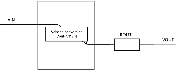 Figure 1. Simplified Model of Charge Pump
This droop characteristics allow current sharing between each module without the need for complex current-sharing circuits or additional external circuitry.
Figure 2 shows a schematic diagram of current sharing based on the droop characteristics. Figure 2 shows the relationship between output voltage and output current (IOUT) when two power supply modules are connected in parallel. The slope of Module 1 and Module 2 in Figure 2 varies depending on the ROUT shown in the previous equation and the wiring layout of the specific module. This slope determines the current flowing between each module. When the ROUT and wiring impedance of both modules and the module temperature are perfectly matched, half of the output current (IOUT/2) flows through each module. On the other hand, if there is a difference in the slope of the droop, the IOUT1 current flows in Module1 and the IOUT2 current flows in Module2, resulting in a state where IOUT1>IOUT/2>IOUT2 as shown in Figure 2. However, Module 1 has a higher current flow than Module 2, resulting in increased losses and heat generation. Because a higher module temperature results in a higher ROUT, the current in Module1 decreases. Therefore, the currents in Module 1 and Module 2 are balanced so that the difference between them is automatically reduced.
In Figure 2, we assumed similar output voltages for each module at no load. However, if there is a difference in output voltages at no load, current cycling occurs between modules. This results in a positive current flow in Module 1 and a negative current flow (reverse current) in Module 2, and the output voltage becomes stable. In this state, current cycling causes unnecessary current to flow, which increases the loss at no load.
MYC0409-NA uses a charge pump, and since the output voltage at no load does not depend on ROUT as described above, the output voltage is approximately the same without adjustment or compensation by trimming.
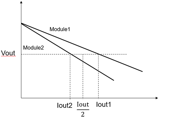 Figure 2 Current Sharing Based on Droop Characteristics
Power Derating in Parallel Operation
The maximum output current in parallel operation is not the rated current for single operation × number of modules in parallel, and power derating occurs. The reason for this is that the output current of each module cannot share the current equally.
The output voltage at no load is approximately the same because VOUT=VIN/4 as described above, but the slope of the droop for each module varies due to variations in the components inside the module and the wiring connecting the modules. Since the slope of the droop varies with module temperature, the power derating must be determined by taking into consideration the mounting environment, heat dissipation structure, and input/output wiring resistance.
Figure 3 shows the equivalent circuit diagram of the resistor components of a system where MYC0409-NA is installed. Figure 3 shows four modules connected in parallel, and ROUT* is the ROUT of each module.
Figure 4 shows the ROUT measurement points of MYC0409-NA. Figure 4 shows that the input and output voltages at measurement are detected in the red frame, and output current is measured outside the module to calculate ROUT.
Rip* and Rop* are the resistor components of the wiring pattern from the power supply and load to the module measurement points shown in Figure 4. The evaluation board used in this article, which is described below, has sufficiently low Rip* and Rop* compared to the ROUT of the module that these values can be ignored. However, Rip* and Rop* can affect current sharing under conditions where incorporating into a distributed power supply system results in longer wiring and for certain copper foil thicknesses and layer configurations on the board. In such cases, these parameters must be taken into account in the calculation.
 Figure 3. Equivalent Circuit Diagram of Resistor Components in System with MYC0409-NA Connected in Parallel
 Figure 4. ROUT Measurement Points
Temperature Coefficient
As mentioned earlier, ROUT is affected by the module temperature. We measured the temperature characteristics of ROUT of MYC0409-NA to confirm the effect of temperature on ROUT. ROUT has a temperature coefficient that is approximately proportional to the module temperature, which varies for each input voltage. There are several factors that contribute to ROUT, such as parasitic resistance of semiconductors and wiring, and bias characteristics of ceramic capacitors. Consequently, the effect on losses depends on the temperature and the voltage applied.
Temperature coefficients obtained from actual measurements are shown in Table 1.
Calculation Formula
In parallel operation, the highest current flows to the module with the lowest sum of ROUT and wiring resistance. The total output current (IOUT_4para) is calculated using the current value of the module with the highest current flow as a rated current of 6 A for single operation.
Assuming the condition that the sum of ROUT1 and wiring resistance is the lowest, the formula for the maximum output current is as follows. This formula determines the output current derating for parallel operation. This is only a formula, and usage should not exceed the rated current of 6 A.
- ROUT*1
- ROUT of each module (TA=25°C)
- R*
- Resistance value of wiring pattern
- K
- Temperature coefficient
- T*
- Temperature of each module
The same formula applies when the number of units operating in parallel is two.
Evaluation Results
The evaluation board used to evaluate current sharing is shown in Figure 5. In this evaluation, current sharing was measured when four MYC0409-NAs were installed on the evaluation board. The current was detected by mounting a current sensing resistor at the output of each module and measuring the current flowing through the resistor. Figure 6 shows the circuit diagram.
Figure 7 shows the current sharing for each input voltage, and Figure 8 shows the current difference from the equally current-shared state (IOUT/4) for each input voltage. The results show that good current sharing of ±3% or less is achieved in the range of load current IOUT=1 A or higher. At light loads, current values are low and temperature compensation is difficult to apply, so there tends to be a difference in current values between modules, but the measurement environment is one factor in this variation of effects. Future work is needed on measurement methods to improve measurement accuracy at light loads, such as the offset of operational amplifiers for current amplification and the accuracy of measuring instruments.
Figure 9 shows the temperature characteristics. The temperature for this evaluation was TA=25°C, and the evaluation was conducted under natural air cooling conditions. Since heat dissipation by heat sinks was not performed in this measurement, the temperature of the two modules in the center, where heat is difficult to escape, increased. If forced-air cooling is performed from CH1 or CH4 in Figure 5, the temperature of the module mounted on the fan side will drop and current will flow more easily. Care should be taken with fan orientation when using forced-air cooling, as forced-air cooling may worsen current sharing between modules.
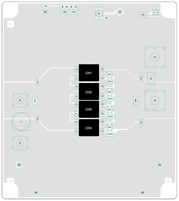 Figure 5. Evaluation Board for MYC0409-NA
114.5 × 101.5 × 1.6mm(4 Layer FR-4)
Outer layer (1, 4) = 2 oz, Inner layer (2, 3) = 1 oz
Figure 6. Evaluation Circuit
Figure 7. Current Sharing for Various Input Voltages
Figure 8. Difference in Output Current for Various Input Voltages
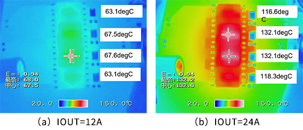 Figure 9. Temperature Characteristics (VIN=48 V, VOUT=12 V)